Apple iPhone 12: The chip advance set to make smartphones smarter
- Posted on
- Comment
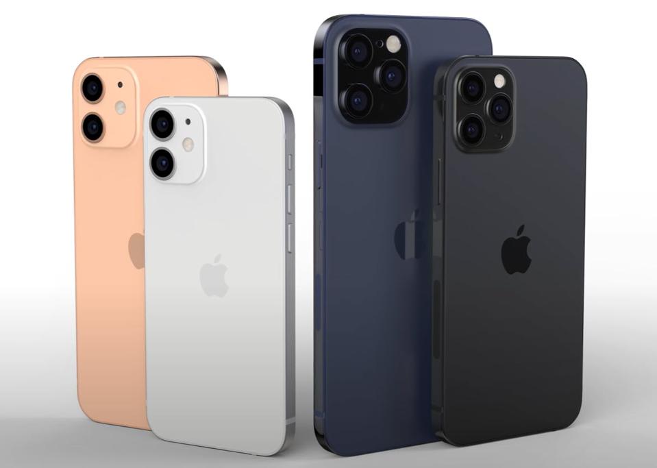
When Apple unveils its new iPhones, expect it to make a big deal of the fact they’re the first handsets in the world to be powered by a new type of chip.
This, we’ll likely be told, will let owners do things like edit 4K video, enhance high-resolution photos and play graphically-intensive video games more smoothly than was possible before while using less battery power.
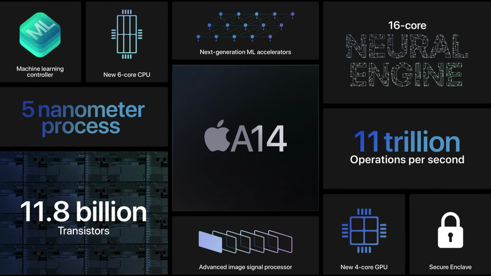
The “five nanometre process” involved refers to the fact that the chip’s transistors have been shrunk down – the tiny on-off switches are now only about 25 atoms wide – allowing billions more to be packed in.
Effectively it means more brain power.
Travel back just four years, and many industry insiders doubted the advance could be delivered soon.
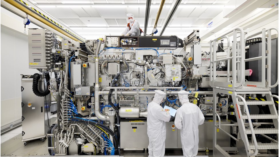
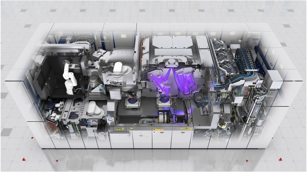
That it has been, is in large part down to the ingenuity of a relatively obscure Dutch company – ASML.
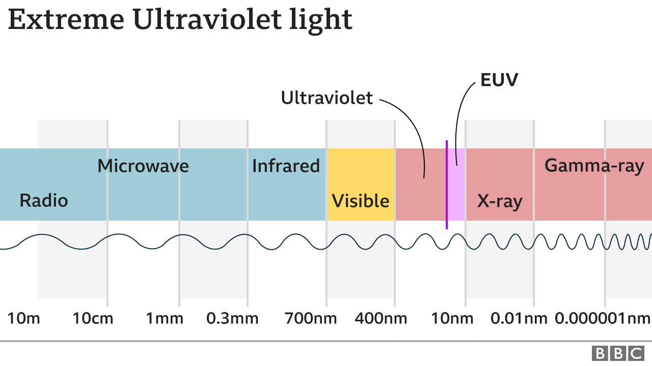
It pioneered a way to carve circuitry patterns into silicon via a process called extreme ultraviolet (EUV) lithography.
Its machines cost a cool $123m (£92m) each, which is high even in relation to other semiconductor industry tools.
But it’s currently the only company making them. And they are still more cost-effective than alternative options, in part because of a low defect rate.
“At such small scales precision is key,” said Dr Ian Cutress, who reports on the sector for Anandtech.
“What they’re doing is akin to hitting a stamp on the surface of Mars with a paper aeroplane.”
ASML likens its technology to making the leap from using a marker pen to a fine-liner.
But rather than ink, it uses what it terms “feeble light” generated via a mind-boggling process.
“We take a molten droplet of tin and we fire a high-power industrial laser onto it, which basically vaporises it and creates a plasma,” explained spokesman Sander Hofman.
“And that plasma shines UV light.
“This all happens 50,000 times a second – so 50,000 droplets get hit – which creates enough light for us to capture with a series of mirrors – the flattest in the world.”
A blueprint of the chip’s design is encoded into the light, he added, by passing it through a mask and then shrinking it with lenses.
It then hits a light-sensitive coating on a silicon wafer, causing the chip’s design to be “printed”.
Only two chip manufacturers have put this to commercial use so far :
- Taiwan Semiconductor Manufacturing Company (TSMC) – sole supplier of the A14 to Apple for its latest iPhones, iPads and Mac computers
- Samsung – which is making a new Qualcomm processor for Android phones, set to be formally unveiled in December
The two firms each own a stake in ASML alongside Intel, which is also expected to start using the tech in 2021.
But one notable competitor has been locked out.
China’s Semiconductor Manufacturing International Corporation (SMIC) reportedly put in an order, but the US government intervened to prevent ASML’s machine being exported on the basis its output might end up in weaponry used by the Chinese military.
SMIC currently lags several generations behind on 14nm chip tech, and experts suggest it would have needed some time to master everything required to move to 5nm.
But the fact it has been blocked from even trying leaves the company and Beijing’s wider ambitions for its chip industry “in a difficult position”, said Jon Erensen from research firm Gartner.
“That is the US’s intention,” he added.

What exactly does 5nm refer to?
A nanometre is one billionth of a metre. That’s roughly the speed a human hair grows every second.
Transistors used to be measured in terms of the width of a part known as their “gate”.
But about a decade ago, a chnage in the way they were designed meant the nanometre reference stopped being tied to a single geometry.
Today the 5nm reference is little more than a marketing term and two foundries using the same designation may offer transistors with different performance.
However, to help imagine how small Apple’s new transistors are, there are about 171 million laid out over every square millimetre.
Another Chinese tech giant, Huawei, has also found itself unable to get its own Kirin 5nm chip designs manufactured as a result of a more recent intervention by the Trump administration.
However, it is expected to shortly reveal it stockpiled a batch made by TSMC for use in its next Mate smartphones, which were manufactured before the Taiwanese firm was forced to end production in September.
Smarter smartphones
All this matters because moving to 5nm is key to making our handsets smarter.
As chips advance, more tasks that used to be sent to remote computer servers for processing can be done locally.
We’ve already seen smartphones become capable of transcribing voice notes and recognising people in photos without the need for an internet connection.
Now even more complex “artificial intelligence” jobs become possible, potentially helping smartphones make better sense of the world around them.
Moving to smaller transistors helps because they use less power than larger ones, meaning they can be run more quickly. On this basis, TSMC has said that its 5nm chips deliver a 15% speed boost over the last 7nm generation while using the same power.
But bigger gains can also be delivered because chip designers get space to create more special sections known as “accelerators”.
“If you have a defined workload – say image processing, audio signal processing, video encoding or cryptography – the maths involved is very well defined,” explained Dr Cutress.
“And you can design the accelerator to do the task as fast as it can or to extend the device’s battery life.”
Apple has already claimed its A14 chip will do machine learning tasks “up to 10 times faster” than the A13.
Expect other smartphone brands to make similar claims as they move to 5nm.
Of course, consumers will be more impressed by life-improving uses of the technology rather than hypothetical speed gains.
But in the years to come, some applications of the gains 5nm and then 3nm tech promise should be become obvious beyond smartphones – smart glasses that don’t look too bulky, smartwatches that last longer between charges, and perhaps affordable self-driving cars.
-BBC
ABOUT: Nana Kwesi Coomson
An Entrepreneur, Corporate Social Responsibility, Corporate Communications Executive and Philanthropist. Editor-in-Chief of www.233times.com. A Senior Journalist with Ghanaian Chronicle Newspaper. An alumnus of Adisadel College where he read General Arts. His first degree is in Bachelor of Arts - Political Science (major) and History (minor) from the University of Ghana. He holds MSc in Corporate Social Responsibility (CSR) and Energy with Public Relations (PR) from the Robert Gordon University in the United Kingdom. He is a 2018 Mandela Washington Fellow who studied at Clark Atlanta University in USA on the Business and Entrepreneurship track.
View all posts by: Nana Kwesi Coomson


 (Selorm) |
  (Nana Kwesi)